

How ASML Got EUV Lithography
And how the US lost it.

This is a crossposting from Brian Potter, the author of the Construction Physics newsletter, a project from the Institute for Progress. Construction Physics features excellent essays about buildings, infrastructure, and industrial technology. You can subscribe here.
Moore’s Law, the observation that the number of transistors on an integrated circuit tends to double every two years, has progressed in large part thanks to advances in lithography: techniques for creating microscopic patterns on silicon wafers. The steadily shrinking size of transistors — from around 10,000 nanometers in the early 1970s to around 20-60 nanometers today — has been made possible by developing lithography methods capable of patterning smaller and smaller features. The most recent advance in lithography is the adoption of Extreme Ultraviolet (EUV) lithography, which uses light at a wavelength of 13.5 nanometers to create patterns on chips.1
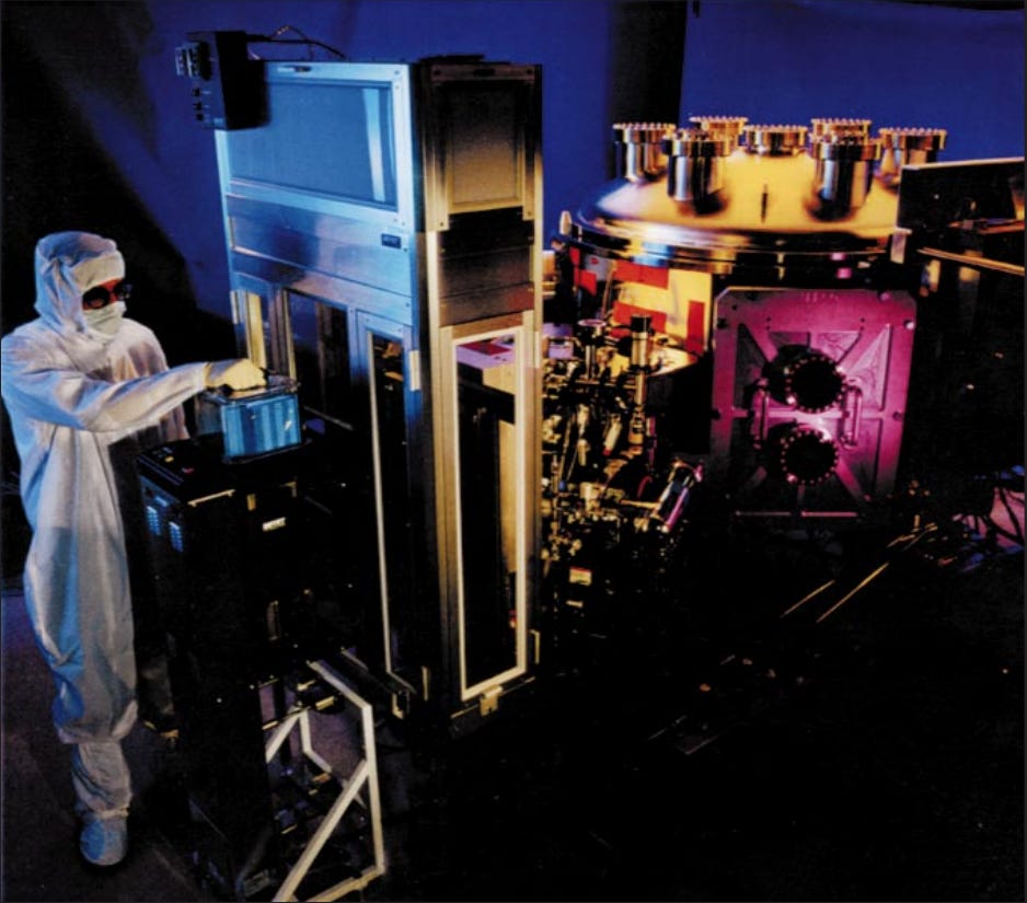
EUV lithography machines are famously made by just a single firm, ASML in the Netherlands, and determining who has access to the machines has become a major geopolitical concern. However, though they’re built by ASML, much of the research that made the machines possible was done in the US. Some of the most storied names in US research and development — DARPA, Bell Labs, IBM Research, Intel, the US National Laboratories — spent decades of research and billions of dollars to make EUV possible.
So why, after all that effort by the US, did EUV end up being commercialized by a single firm in the Netherlands?
How semiconductor lithography works
Briefly, semiconductor lithography works by selectively projecting light onto a silicon wafer using a mask. When light shines through the mask (or reflects off the mask in EUV), the patterns on that mask are projected onto the silicon wafer, which is covered with a chemical called photoresist. When the light strikes the photoresist, it either hardens or softens the photoresist (depending on the type). The wafer is then washed, removing any softened photoresist and leaving behind hardened photoresist in the pattern that needs to be applied. The wafer will then be exposed to a corrosive chemical, typically plasma, removing material from the wafer in the places where the photoresist has been washed away. The remaining hardened photoresist is then removed, leaving only an etched pattern in the silicon wafer. The silicon wafer will then be coated with another layer of material, and the process will repeat with the next mask. This process will be repeated dozens of times as the structure of the integrated circuit is built up, layer by layer.
Early semiconductor lithography was done using mercury lamps that emitted light of 436 nanometers wavelength, at the low end of the visible range. But as early as the 1960s, it was recognized that as semiconductor devices continued to shrink, the wavelength of light would eventually become a binding constraint due to a phenomena known as diffraction. Diffraction is when light spreads out after passing through a hole, such as the openings in a semiconductor mask. Because of diffraction, the edges of an image projected through a semiconductor mask will be blurry and indistinct; as semiconductor features get smaller and smaller, this blurriness eventually makes it impossible to distinguish them at all.
The search for better lithography
The longer the wavelength of light, the greater the amount of diffraction. To avoid eventually running into diffraction limiting semiconductor feature sizes, in the 1960s researchers began to investigate alternative lithography techniques.
One method considered was to use a beam of electrons, rather than light, to pattern semiconductor features. This is known as electron-beam lithography (or e-beam lithography). Just as an electron microscope uses a beam of electrons to resolve features much smaller than a microscope which uses visible light, electron-beam lithography can pattern features much smaller than light-based lithography (“optical lithography”) can. The first successful electron lithography experiment was performed in 1960, and IBM extensively developed the technology from the 1960s through the 1990s. IBM introduced its first e-beam lithography tool, the EL-1, in 1975, and by the 1980s had 30 e-beam systems installed.
E-beam lithography has the advantage of not requiring a mask to create patterns on a wafer. However, the drawback was that it’s very slow, at least “three orders of magnitude slower than optical lithography”: a single 300mm wafer takes “many tens of hours” to expose using e-beam lithography. Because of this, while e-beam lithography is used today for things like prototyping (where not having to make a mask first makes iterative testing much easier) and for making masks, it never displaced optical lithography for large-volume wafer production.
Another lithography method considered by semiconductor researchers was the use of X-rays. X-rays have a wavelength range of just 10 to 0.01 nanometers, allowing for extremely small feature sizes. As with e-beam lithography, IBM extensively developed X-ray lithography (XRL) from the 1960s through the 1990s, though they were far from the only ones. Bell Labs, Hughes Aircraft, Hewlett Packard, and Westinghouse all worked on XRL, and work on it was funded by DARPA and the US Naval Research Lab.
For many years X-ray lithography was considered the clear successor technology to optical lithography. In the late 1980s there was concern that the US was falling behind Europe and Japan in developing X-ray lithography, and by the 1990s IBM alone is estimated to have invested more than a billion dollars in the technology. But like with e-beam lithography, XRL never displaced optical lithography for large-volume production, and it’s only been used for relatively niche applications. One challenge was creating a source of X-rays. This largely had to be done using particle accelerators called synchrotrons: large, complex pieces of equipment which were typically only built by government labs. IBM, committed to developing X-ray lithography, ended up commissioning its own synchrotron (which cost on the order of $25 million) in the late 1980s.
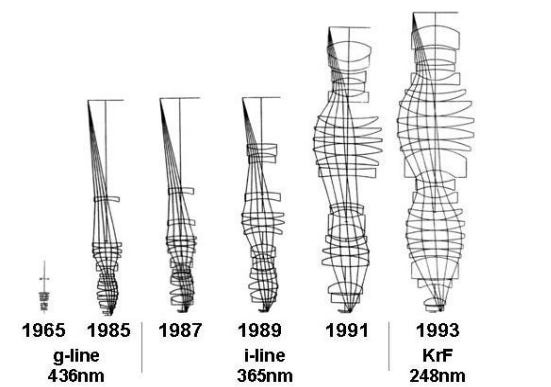
Part of the reason that technologies like e-beam and X-ray lithography never displaced optical lithography is that optical lithography kept improving, surpassing its predicted limits again and again. Researchers were forecasting the end of optical lithography since the 1970s, but through various techniques, such as immersion lithography (using water between the lens and the wafer), phase-shift masking (designing the mask to deliberately create interference in the light waves to increase the contrast), multiple patterning (using multiple exposures for a single layer), and advances in lens design, the performance of optical lithography kept getting pushed higher and higher, repeatedly pushing back the need to transition to a new lithography technology. The unexpectedly long life for optical lithography is captured by Sturtevant’s Law: “the end of optical lithography is 6 – 7 years away. Always has been, always will be.”
The rise of EUV
In the early 1980s, Hiroo Kinoshita, a researcher at Japan’s Nippon Telephone and Telegraph (NTT), was researching X-ray lithography, but was becoming disillusioned by its numerous difficulties. The X-ray lithography technology being used was known as “X-ray proximity lithography” or XPL. Whereas in optical lithography light passed through a lens to reduce the image size projected onto the silicon wafer, because no known materials could make a reduction lens for X-rays, X-rays were projected directly onto the wafers without any sort of lens reduction. In part because of the lack of reduction — which meant that any imperfections in the mask wouldn’t be scaled down when projected onto the wafer — making masks for XPL proved exceptionally difficult.
However, while it’s not possible to focus X-rays with a lens, it is possible to reflect certain X-ray wavelengths with a mirror. A normal mirror will only reflect X-rays at very shallow angles, making it very hard to use them for a practical lithography system (the requirement of a shallow angle would make such a system gigantic); at steeper angles, X-rays will simply pass through the mirror. However, by constructing a special mirror from alternating layers of different materials, known as a “multilayer mirror,” light near the X-ray region of the spectrum can be reflected at much steeper angles. Multilayer mirrors use layers of different materials with different indices of refraction (how much light bends when entering it) to create constructive interference — each layer boundary reflects a small amount of light, which (when properly designed) adds together with the reflection from the other layers. (Anti-reflective coatings use a similar principle, but instead use multiple layers to create destructive interference to eliminate reflections.)
The first multilayer mirrors that could reflect X-rays were built in the 1940s, but they were impractical because the mirrors were made from gold and copper, which quickly diffused into each other, degrading the mirror. But by the 1970s and 80s, the technology for making these constructive interference-creating mirrors had dramatically improved. In 1972 researchers at IBM successfully built a 10-layer multilayer mirror that reflected a significant fraction of light in the 5 to 50 nanometer region, and in 1981 researchers at Stanford and the Jet Propulsion Laboratory built a 76-layer mirror from alternating layers of tungsten and carbon. A few years later researchers at NTT also successfully built a multilayer tungsten and carbon film, and based on their success Kinoshita, the researcher at NTT, began a project to leverage these multilayer mirrors to create a lithography system. In 1985 his team successfully projected an image using what were then called “soft X-rays” (light in roughly the 2 nanometer to 20 nanometer range) reflected off of multilayer mirrors for the first time. That same year, researchers at Stanford and Berkeley published work showing that a multilayer mirror made from molybdenum and silicon could reflect a very large fraction of light near the 13 nanometer wavelength. Because X-rays in a lithography tool will bounce off of multiple mirrors (a modern EUV tool might have 10 mirrors), reflecting a large portion of them is key to making a lithography tool practical; too little reflection and the light will be too weak by the time it reaches the wafer.2
Initially people in the field were skeptical about the prospects of a reflective X-ray lithography system. When presenting this research in Japan, Kinoshita noted that his audience was “highly skeptical of his talk” and that they were “unwilling to believe that an image had actually been made by bending X-rays.” The same year, when Bell Labs researchers suggested to the American government that soft X-rays with multilayer mirrors could be used to create a lithography system, they received an “extremely negative reaction”; reviewers argued that “even if each of the components and subsystems could be fabricated, the complete lithography system would be so complex that its uptime would be negligible.” When researchers at Lawrence Livermore National Lab, after learning of Kinoshita’s work, presented a paper on their own soft X-ray lithography work in 1988, reception was similarly negative. One paper author noted that “You can’t imagine the negative reception I got at that presentation. Everybody in the audience was about to skewer me. I went home with my tail between my legs…”
Despite the negative reactions, work on soft X-ray lithography continued to advance at NTT, Bell Labs, and Livermore. Kinoshita’s research group at NTT designed a new two-mirror soft x-ray lithography system, and used it to successfully print patterns with features 500 nanometers wide. When presenting this work at a 1989 conference in California, a Bell Labs researcher named Tania Jewell became extremely interested, and “deluged” Kinoshita with questions. The next year, Bell Labs successfully printed a 50 nanometer pattern using soft X-rays. The 1989 conference, and the meeting between NTT and Bell Labs, has been called the “dawn of EUV.”
Work on soft X-ray lithography continued in the 1990s. Early soft X-ray experiments had been done with synchrotron radiation, but a synchrotron would be difficult to make into a practical light source for high-volume production, so researchers looked for alternative ways to generate soft X-rays. One strategy for doing this is to heat certain materials, such as xenon or tin, enough to turn them into a plasma. This can be done using either lasers (creating laser produced plasma, or LPP) or electrical currents (creating discharge produced plasma, or DPP). Development of LPP power sources began in the 1990s, but creating such a system was enormously difficult. Turning material into a plasma generated debris which reduced the life of the extremely sensitive multilayer mirrors, and a “great deal of effort [was] put into designing and testing a variety of debris minimization schemes.” One strategy that proved to be very successful was to minimize the amount of debris by creating a “mass limited target”: minimizing the amount of material to be heated into plasma by emitting it as a series of microscopic droplets. Over time, these and other strategies allowed for longer and longer mirror life.
Another major challenge was manufacturing sufficiently precise multilayer mirrors. In 1990, mirrors could be fabricated with at most around 8 nanometers of precision, but a practical soft X-ray lithography system demanded 0.5 nanometer precision or better. NTT had obtained its first multilayer mirrors from Tinsley (the US firm that had built the ultra-precise mirrors for the Hubble Space Telescope), and with NTT’s encouragement Tinsley was able to fabricate mirrors of 1.5 to 1.8 nanometer accuracy in 1993. Similar work on mirror accuracy was done at Bell Labs (with assistance from researchers at the National Institute of Standards and Technology), and during the 1990s the precision of multilayer mirrors continued to improve.
As work on it was proceeding, a change in name for soft X-ray technology was suggested. “Soft X-ray” was thought to be too close to X-ray proximity lithography, which worked on different principles (ie: it had no mirrors) and had developed a negative reputation thanks to its difficult development history. So in 1993 the name was changed to Extreme Ultraviolet Lithography, or EUV. The wavelengths used for soft X-rays were at the very bottom of the ultraviolet spectrum, and the name created associations with “Deep Ultraviolet Lithography” (DUV), a lithography technique based on 193-nanometer light, which was then being used successfully.
Organizational momentum behind EUV continued to build. In the early 1990s Sandia National Labs, using technology developed for the Strategic Defense Initiative, partnered with Bell Labs to demonstrate a soft X-ray lithography system using a laser produced plasma. In 1991, Japanese corporations Nikon and Hitachi also began to research EUV technology. That same year, the Defense Advanced Research Projects Agency (DARPA) began to fund lithography development via its Advanced Lithography Program, and by 1996 Sandia National Labs and Lawrence Livermore lab had committed around $30 million to EUV development (with a similar amount contributed by several private companies). In 1992, Intel committed $200 million into the development of EUV, most of which funded research work at Sandia, Livermore and Bell Labs. In 1994, the US formed the National EUV Lithography Program, made up of researchers from the national labs (Livermore, Berkeley, and Sandia), and led by DARPA and the DOE.
EUV-LLC
In 1996, Congress voted to terminate DOE funding for EUV research. Without funding to keep the research community together, the national lab researchers would be reassigned to other tasks, and much of the knowledge around EUV might dissipate. At the time, there were still numerous difficulties with EUV, and it was far from obvious it would be the successor lithography technology: a 1997 lithography task force convened by SEMATECH (a US semiconductor industrial consortium) ranked EUV last of four possible technologies behind XPL, e-beam lithography, and ion projection lithography.
Despite the uncertainty, Intel placed a bold bet on the future of EUV, and stepped in with around $250 million in funding to keep the EUV research program alive. It formed a consortium known as EUV-LLC, which contracted with the Department of Energy to fund EUV work at Sandia, Berkeley, and Livermore national labs. Other major US firms, including Motorola, AMD, IBM, Micron also joined the consortium, but Intel remained the largest and most influential shareholder, the “95% gorilla.” Following the creation of EUV-LLC, Europe and Japan formed their own EUV research consortiums: EUCLIDES in Europe and ASET in Japan.
When EUV-LLC was formed, US lithography companies had been almost completely forced out of the global marketplace. Japanese firms Nikon and Canon held a 40% and 30% share of the market, respectively, and third place was held by an up-and-coming Dutch firm called ASML, which held 20% market share. The members of EUV-LLC, not least Intel, wanted a major foreign lithography firm to join the consortium to help ensure EUV became a global standard However, the prospect of funding the development of advanced semiconductor technology, only to hand that technology over to a national competitor (especially a Japanese competitor who had so recently been responsible for decimating the US semiconductor industry), wasn’t an easy sell. Nikon declined to participate in EUV-LLC in part due to the resulting controversy, and Canon was ultimately prevented from joining by the US government.
ASML, however, was different. Being located in the Netherlands, it was considered “neutral ground” in the semiconductor wars between the US and Japan. Intel, whose main concern was that it could itself get access to the next generation of lithography tools regardless of who produced them, strongly advocated that ASML be allowed to procure a license. (One executive at the US lithography company Ultratech Stepper complained that Intel had “done everything in their power to give the technology to ASML on a silver platter.”) In 1999, ASML was allowed to join EUV-LLC and gain a license for its technology, provided that it used a sufficient quantity of US components in the machines it built and opened a US factory — conditions that it never met.
Left outside of the EUV-LLC consortium, Nikon and Canon never successfully developed EUV technology. And neither did any US firms. Silicon Valley Group, a US lithography tool maker which had licensed EUV technology, was bought by ASML in 2001, and Ultratech Stepper, another US licensee, opted not to pursue it. ASML, in partnership with German optics firm Carl Zeiss, became the only lithography firm to take EUV technology across the finish line.
Conclusion
Over the next several years, EUV-LLC proved to be a huge success, and when the program ended in 2003, it had met all of its technical goals. EUV-LLC had successfully built a test EUV lithography tool, made progress on both LPP and DPP light sources, developed masks that would work with EUV, created better multilayer mirrors, and filed for over 150 patents. Thanks in large part to Intel’s wager, EUV would ultimately become the lithography technology of the future, a technology that would entirely be in the hands of ASML.
This future took much longer to arrive than expected. When the EUV-LLC program concluded in 2003, US semiconductor industry organization SEMATECH stepped in to continue funding work on commercialization. ASML shipped its first prototype EUV lithography tool in 2006, but with very weak DPP power sources. A US company, Cymer (later acquired by ASML), was developing a better power source using a laser-produced plasma, but working out the problems with it took years and required further investment from Intel. Making defect-free EUV masks proved to be similarly difficult. EUV development proved to be so difficult that ASML ultimately required billions of dollars in investment from TSMC, Samsung, and Intel to fund its completion: the three companies invested $1 billion, $1 billion, and $4 billion, respectively in ASML in 2012 in exchange for shares of the company. ASML didn’t ship its first production EUV tool until 2013, but development work on things like the power source (often funded by the US) continued for years afterwards. Intel, worried about the difficulties of getting EUV into high-volume production, made the ultimately disastrous decision to try and push optical lithography technology one more step for its 10 nanometer process.
But today, after decades of development, EUV has arrived. TSMC, Intel, and Samsung, the world’s leading semiconductor fabricators, are all using EUV in production. And they are all using lithography tools built by ASML for it.
An important takeaway from the story of EUV is that developing a technology that works, and successfully competing with that technology in the marketplace, are two different things. Thanks to contributions from researchers around the world, including a who’s who of major US research organizations — DARPA, Bell Labs, the US National Labs, IBM Research — EUV went from unpromising speculation to the next generation of lithography technology. But by the time it was ready, US firms had been almost entirely forced out of the lithography tools market, leaving EUV in the hands of a single European firm to take it across the finish line and commercialize.
Modern semiconductor processes often have names that imply smaller sizes — TSMC’s 7 nm node, Intel’s 10 nm node — but these are essentially just names that don’t correspond with actual feature sizes.
Definitions for what light is considered to be “soft x-ray” don’t seem especially consistent. One article notes that “the terms soft X-ray and extreme ultraviolet aren’t well defined.”
 | A guest post by
|